LAUGHTON ELECTRONICS

Cheap Video à la Lancaster and the back story re: my KIM-1

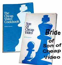
At the dawn of the microcomputer era, back in the days of the 8080 and the Motorola 6800, a certain Pioneer of the Art published plans for a remarkable microprocessor interface. Don Lancaster published a series of books, including The Cheap Video Cookbook and Son of Cheap Video. These explain an unorthodox technique that allows rudimentary microcomputers like the Altair and the KIM-1 to generate video output. The novelty of Lancaster's approach left an impression on me, and I took to heart an important lesson: sometimes the most expedient way to solve a problem is to "lie" to the machine!

Incidentally, the title of my KimKlone article is a grateful acknowledgment to Mr Lancaster and his humorous style:
  (Lancaster's book:)  Cheap Video Cookbook
  (Lancaster's book:)  Son of Cheap Video
  (my spin-off article:)  Bride of Son of Cheap Video

Cheap Video and Lying To the Machine

Lancaster book covers


The lowdown on Cheap Video.


Cheap Video is a means of outputting video without the need for DMA hardware or a Video Controller chip. Instead what's used is programmed I/O. The video is generated as the output of an actual program running on the computer. This would ordinarily be impossible (due to the very high data rate required), but Cheap Video has a trick up its sleeve, something devious done in hardware to fool the CPU. But first let's look at the software.

At the heart of the video program is a loop. Each iteration of the loop outputs one row of pixels, corresponding to one horizontal sweep (or "scan") of the CRT monitor. Each iteration begins with the CPU making a Jump To Subroutine (JSR) to some address in a portion of memory defined as the video buffer. Rather than the pixel data, what the CPU "sees" in the buffer is a seemingly pointless subroutine composed of dozens of NOPs then an RTS. Naturally the CPU follows orders and executes these instructions. What's noteworthy is that the address bus increments steadily as the NOPs execute. In other words the CPU's Program Counter (PC) spends a few dozen cycles behaving like a 16-bit counter. And, it is counting its way through a portion of the video buffer.

Following the RTS the spell is broken; we return to reality and procede through the rest of the loop. The CPU outputs a horizontal sync pulse, computes a new address for the next JSR to the video buffer, and then the loop reiterates. There's no exit until there have been enough scans (horizontal lines) to refresh the entire screen from top to bottom. This completes one frame.

To produce a continuous succession of frames, an outer loop outputs the Vertical Sync pulse and rolls the JSR address back to its top-of-the-screen value before the inner loop commences again. Two incidental points: this description applies to bit-mapped displays. If a Character Generator ROM is used then each pixel line is part of a row of character cells, and the inner loop requires extra details I won't describe. Another option not discussed here is interlacing.

The devious hardware hoax mentioned earlier is what causes the CPU to see the buffer area as containing NOPs rather than what's really there (the video data). Here's how it's done, and why:

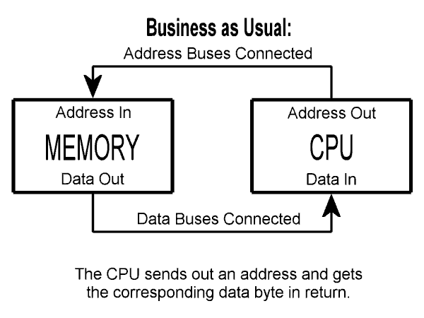
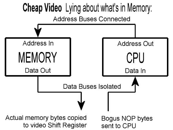
Usually when a CPU sends out an address, memory will faithfully reply with the byte stored at that address. But with Cheap Video a major connection — that between the data buses — gets temporarily severed. This lets Cheap Video "lie" about what's in memory. (See the diagrams on the left, Business as Usual and Cheap Video.) During each scan, the bytes fetched onto the memory data bus do not get relayed back to the CPU's data bus. Instead, the bytes of memory data (ie; the pixel data we needed to fetch) get merrily shipped off to the video display. Meanwhile, some Cheap Video flimflam logic feeds the CPU bus a brazen fabrication, a persistent NOP (and eventual RTS) which appear to reside at the addresses actually containing data.

Lancaster realized that a microprocessor is easily capable of reading 32 or more bytes in a row, even though conventional processing of memory variables can only proceed sporadically and in much smaller chunks. But prolonged sequences of memory reads do occur as the chip fetches the bytes of its program. Broadly speaking we can say that, if there are no branches in a program and no accesses to memory variables, sequential reads for instruction fetching will continue indefinitely. Therefore NOPs yield the desired "scan" behavior: an extended sequence of back-to-back reads of ascending memory locations. The CPU unwittingly mimics a 16-bit counter or a DMA controller, with its address bus outputting an ascending 16-bit count.

I am indebted to Mr Lancaster for the lesson I learned from Cheap Video, namely that a microprocessor can readily be manipulated by hardware tricks in order to produce unusual behaviors that are useful. The KimKlone, of course, relies very heavily on this principle.


my KIM (the original mashup) and its mutant spawn, the KimKlone

My very first computer was a KIM-1 — the classic, 1-MHz 6502 board from MOS Technology. I hadn't had it long before I added some extra RAM (2114's), a pair of 6522's, an ASCII keyboard & a paper tape reader and, of course, Cheap Video. But around 1980 I switched the focus from video to memory-space expansion. The reason? On the surplus market I'd acquired a DRAM board of 128K capacity!   I was agog; I felt hypoxemic. This utterly outclassed my previous expansion of 8K! And of course it was twice as much as the processor could address.

I decided to down-rate the new board to 112K, which allowed the new memory, the pre-existing memory and the I/O space all to reside within 128K. Then I devised a circuit which recognized some of the undefined aka "illegal" 65c02 opcodes and used them as cues to direct access between "this" bank and "the other" bank. As with the KimKlone (which came later), the banks were a full 64K in size. This contrasts sharly with conventional expansion schemes, which are restricted to a comparatively small "window" (eg, 16K) into the expanded space. Bank switches were impemented as transient events lasting less than one instruction cycle; my new circuitry had to manage its task on a bus cycle by bus cycle basis.

If I recall correctly, the deal with my KIM was that each illegal op-code of the pattern xxxxx011 would cause the upper, don't-care bits (the xxxxx) to select one of thirty-two 8-bit patterns held in a TTL PROM, and the selected pattern was parallel- loaded into a shift register and regurgitated serially. The xxxxx011 op-code acted as a prefix instruction, and the shift register would trot out the corresponding pattern, one bit per cycle, while the following instruction — the target of the prefix — executed. The target would be a normal 65xx memory reference instruction such as INC Absolute, STA Indirect, CMP Indirect-Y or whatever. The shift register's serial output toggled a flip-flop feeding A16, the most-significant address line. Typical timing patterns caused A16 to flip from one 64K bank to the other for a single bus cycle only, exactly during the time the target instruction performed its fetch or store. (Read-Modify-Write instructions used patterns that produced a three-cycle bank switch.) There were other capabilities as well: for instance you could JMP to the alternate bank and stay there, or do a Far JSR and later a Far RTS. The exact details escape me. But the 65c02's 64K address limit was transcended by using undefined op-codes as prefixes to specify Far addressing for legacy instructions.

The arrangement I've described was perfectly functional, but a more elegant solution would be to infer timing information directly from the target op-code. The KIM circuit didn't even sample the target instruction; its behavior depended solely on the prefix. So, instead of just a few prefixes, a few sets of prefixes had to be made available, with members of each set identical except in regard to timing. That's how I was able to match the timing of the CPU as it executes different target instructions using different address modes. It seemed a shame to use all those undefined op-codes so inefficiently, but with the KIM it didn't really matter because there was nothing else that needed to be controlled. Later the KimKlone, a "clean sheet of paper" design, pushed the envelope a great deal further. See KimKlone Short Summary

visit
LAUGHTON
ELECTRONICS
Home
Commercial& Manufacturing
Stage&Studio
Laboratory&OEM
copyright notice (Jeff Laughton)