|
|
What
Is It?
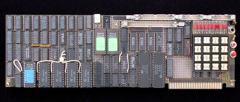
It's a
microcomputer with a cmos 6502 and a coprocessor
— ie; off-chip logic capable
of interpreting the instruction stream.
What Does The
Coprocessor Do?
It assimilated the
6502!
The collective Programming Model has 6
new registers and 44 new
instructions, including NEXT (as used by Forth). The new instructions
run at full speed, and it's all transparent from an assembly programmer's point of view. In
other words, no
difference between native and newly minted instructions.
One main feature is KimKlone's 24-bit address
space. That's been done before, but this implementation preserves
most of the speed of the processor. It's fast because:
- the extended addressing is part of the instruction set. There's no MMU to spoon-feed.
- memory is organized as banks of 64K (not a fraction thereof, such as 16K)
Units of 64K make it easy to treat the entire memory as a linear, 16 MB space,
and to walk through it with simple pointer arithmetic. This opens the door to a modest range of "big data" applications — tasks which would cause
most expanded-memory 8-bit machines to hit the wall. They suffer an order-of-magnitude
speed disadvantage simulating a linear space.
How Does It Work?
Most
of the control
signals originate as microcode fetched from an EPROM array.
The microcode runs on a state machine that's clocked in lock-step with
the CPU. (One state machine cycle = one CPU cycle = one bus cycle.)
The CPU directs instruction fetching. Simultaneous execution by it and
the state machine determines the result.
Bank addresses are stored and retrieved from a group of 74HC670's
which form a small, multi-port register file. One of the read ports connects
to the address bus, driving A23-A16. These new address
lines — and A15-A0 directly from the 65C02 — are what address
the 16 MByte space. The register file also connects to the data bus,
allowing bank addresses to be loaded and recalled. Specific instructions are
provided for this, an arrangement that's more direct than I/O operations on an MMU. It also allows
registers A, X and Y to remain undisturbed.
Although the coprocessor has its own registers, it doesn't
actually compute anything. It's more like an exo-skeleton for the 65C02.
Devices such as the register file connect to the data bus and can be instructed to update themselves from it.
Sometimes they drive the bus when the CPU thinks it's reading data (or even
an instruction operand) from memory! Opcodes get edited, too. Some of the 46 undefined (aka illegal) 65C02
opcodes get replaced with substitutes before they reach
the CPU. Others are used "as is" — they cause the CPU to generate addresses, which
makes them vitally useful. When an illegal opcode is replaced the
substitute may be either another illegal opcode, a normal instruction or a NOP.
But these details are invisible; the programmer
simply has 44 new instructions available (for a total of 254).
What Are
The New Instructions and Registers?
- instructions that load and save the four bank addresses
cued up in the register file
- instructions that actually output a bank address onto A23-A16 (often on a transient basis)
- miscellaneous
The Current
Code Pointer, aka CCP, tends to dominate. It is the
default for readout to the high address lines A23-A16, and it prevails
for the majority of bus cycles, including those for code access and those for Near
data accesses — ie, access within the Current 64K bank. The other three words in the '670 register file appear to
the programmer as Data Pointer
registers DP0, DP1 and DP2.
Three single-byte prefix instructions are
associated with DP0, DP1 and DP2. A Far data access usually takes the
form of a prefix followed by an ordinary 65C02 instruction (eg: INC Absolute, CMP Indirect,Y etc).
At run-time the coprocessor makes note of the prefix and the CPU just steps over it. Next comes the target
instruction, and, as usual, off-chip logic co-executes every cycle. This includes
the extra cycles for zero-page indirection and other variations. Ultimately DP0, DP1 or
DP2 is read out "on cue" for the data transfer which is the final cycle of the
instruction (final three cycles for
Read-Modify-Write). All
of the CPU's 64K possible addresses are re-mapped by the bank switch. Then CCP is
re-selected for A23-A16, an opcode fetch occurs, and the program proceeds without missing a beat. Almost
all instructions and address modes can use the prefixes and thus become
Far. Considering all the combinations, you
could say there are hundreds of new instructions, not
just 44.
The prefixes provide a flexible overall
mechanism, but there are some specialized provisions as well.
Six of the most frequently used forms of Far LDA and Far STA have their
own unique opcodes,
thus eliminating the one byte, one cycle overhead of a prefix. Specific
opcodes are also provided for Far JMP,
Far
JSR and Far RTS. These
instructions include an operation that exchanges CCP and DP2 — and, because
CCP is updated, a new 64K bank becomes the default.
Happily, this does not imply alternative zero-pages and stacks!
The default doesn't apply to stack and zero-page cycles; microcode always directs these accesses to bank zero.
Data Pointer registers DP0, DP1 and DP2 load themselves, responding
to specific opcodes that can select Immediate, Absolute, Z-pg or Z-pg, X address mode.
These three registers can also be pushed and pulled from stack. CCP can only be pushed.
Altogether there are 34 instructions for performing Far jumps, Far data accesses, and for loading and saving bank
addresses.
Miscellaneous instructions and registers
A few highlights from this disparate group are as follows. The SCAN instruction forces the
CPU to rapidly read a long string of bytes from memory, as part of a program that
outputs video. W is a 16-bit register readable in zero-page, one of whose functions is double-indexed
addressing. This involves W capturing the Effective
Address of certain instructions coded with the 6502's (Z-pg,X) mode and
making the EA available in Z-pg. Therefore it's possible to follow the (Z-pg,X)
instruction with one using (W),Y and the result of the two-instruction sequence is
(Z-pg,X),Y mode. It's equivalent to using X to index to a pointer,
fetching the pointer, then indexing again into a data array. This is not so unusual, given that even a 16-bit word (2 bytes) constitutes an array.
Double-indexed addressing accelerates Forth mainstays such as @ and ! (fetch and store).
IP is a
16-bit register whose most notable function
is as a pointer
for the JMP((IP++)) instruction. This double-indirect jump
with post-increment
is a hardware realization of Forth's ubiquitous NEXT
operation. Hardware
NEXT has quadruple
the speed of the code sequence it replaces.
Overall Forth program speed increases
by about 90%.
Conclusion
KimKlone's CPU and
the off-chip accessories function as a unified
whole, much the same as a monolithic device created in a
wafer fab. The design is notable for introducing major features
despite the limitations of a legacy Programming Model and even legacy
silicon.
The linear memory organization allows efficient
manipulation of objects larger than 64K — a
capability which is absent
from commercial 6502 microcomputers and from microprocessors such as
the MOS 6509 and the Hudson Soft 6280
and which, in retrospect, is more suggestive
of the WDC 65816.
(The KK was created shortly after but without any influence from the
65816.)
|
|
")